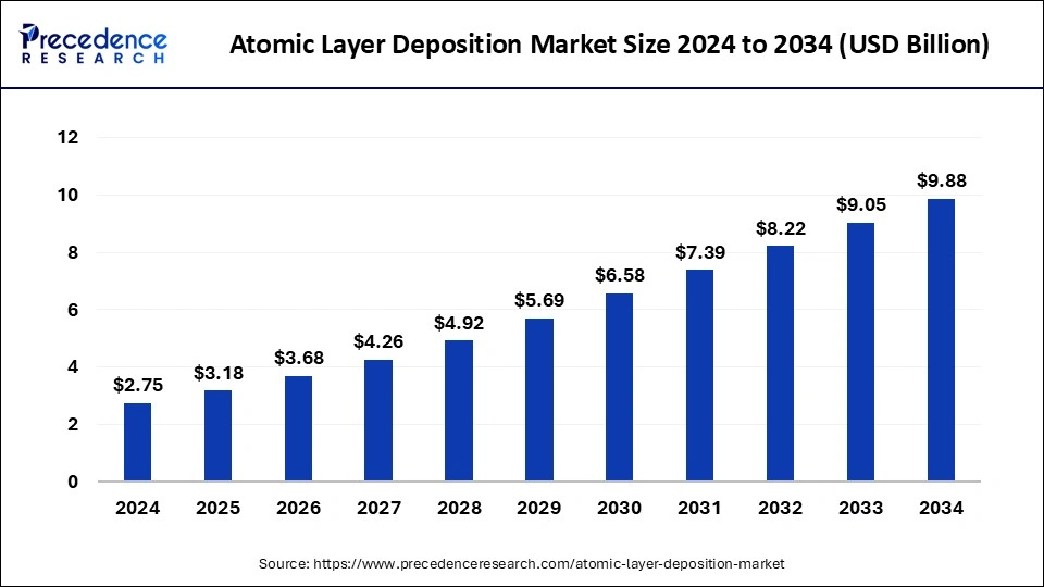
Atomic Layer Deposition Market Size Forecast to Reach USD 9.88 Billion by 2034 Amid Rising Semiconductor and Energy Applications
According to Precedence Research, the global atomic layer deposition market size will grow from USD 3.18 billion in 2025 to nearly USD 9.88 billion by 2034, with an expected CAGR of 13.42% from 2025 to 2034. The growing semiconductor manufacturing and trend of miniaturization of electronics drive the market growth.
Ottawa, Sept. 15, 2025 (GLOBE NEWSWIRE) -- The global atomic layer deposition market size was valued at USD 2.75 billion in 2024 and is forecasted to reach nearly USD 9.88 billion by 2034. In terms of annual growth, the market is expected to expand at a strong CAGR of 13.42% from 2025 to 2034.
Atomic Layer Deposition Market Key Takeaways
- In terms of revenue, the global atomic layer deposition market is projected to be worth USD 3,180 million in 2024.
- Middle East & Africa contributed the largest market share of 66.95% in 2024.
- North America region is growing at a double-digit CAGR between 2025 and 2034.
- By product, aluminium oxide segment held the major market share of 32.63% in 2024.
- By Application, the semiconductors segment accounted for the highest market share of 41.46% in 2024.
What is the Atomic Layer Deposition Market and Why is it Important?
The atomic layer deposition (ALD) market refers to the industry built around using ALD technology for creating ultra-thin films with atomic-level accuracy. Instead of being just a scientific method, ALD has become a commercial tool that industries rely on for producing coatings with unmatched precision and reliability.
This market is important because ALD allows manufacturers to produce highly uniform, defect-free coatings that improve performance, efficiency, and durability. From semiconductors and energy storage to medical devices and protective coatings, ALD technology supports innovation in several fields. As demand grows for smaller, faster, and longer-lasting products, the ALD market is playing a central role in making these advancements possible.
Latest Private Sector Investments in Atomic Layer Deposition:
- Chipmetrics (Finland) raised €2.4 million in seed funding led by High-Tech Gründerfonds and OCCIDENT (also Innovestor, REDSTONE, and BALD Engineering) to commercialize their metrology tools (PillarHall®) for measuring thin-film conformity in ALD processes in January 2024. (venturebanc.com)
- In July 2024, Kalpana Systems (Netherlands) raised about €3.5 million from corporate and institutional investors (including packaging company SIG and its corporate VC arm SIG InnoVentures) plus government support to develop roll-to-roll spatial ALD tools for solar PV, OLEDs, batteries, and packaging. (pv magazine International)
- SparkNano (Netherlands) secured €5.5 million in a funding round (led by ALIAD, plus Somerset Capital Partners, Invest-NL, etc.) to scale up its spatial ALD equipment aimed at energy applications, including solar cells, green hydrogen, fuel cells, and batteries. These investments were made in November 2022. (Silicon Canals+1)
- Forge Nano (via its merger with ALD NanoSolutions) raised US$20 million from corporates including Volkswagen, LG Technology Ventures, Mitsui Kinzoku Trading, SBI Investment, etc., to expand manufacturing/materials capabilities using ALD for applications such as energy storage, thin films, and electronics. (Global Venturing)
- Genus, Inc. (USA) raised US$7.8 million via a private placement of convertible notes (plus a smaller investor contribution) to push forward the commercialization of their ALD technologies (inventory, customer support, sales, etc.). (EE Times+1)
High-Tech Innovations Driving Atomic Layer Deposition Market Toward Strong Growth – Browse Detailed Insights @ https://www.precedenceresearch.com/atomic-layer-deposition-market
Types of Atomic Layer Deposition
| Types | Description | Applications |
| Thermal ALD | The deposition of one atomic layer of thin films at a time using heat is called thermal ALD. |
|
| Plasma-Enhanced ALD | The deposition of plasma films layer by layer in cycles is called PE-ALD. |
|
| Photo-Assisted ALD | It uses ultraviolet light to enhance film quality and accelerate chemical reactions. |
|
Atomic Layer Deposition Market Trends
-
Rising Demand in Semiconductor Manufacturing: The ongoing miniaturization of semiconductor devices (especially below 5nm nodes) is driving strong demand for ALD due to its precision in depositing ultra-thin, conformal films.
-
Growth in 3D NAND and Advanced Memory Devices: ALD is critical for fabricating complex 3D memory structures, such as 3D NAND and DRAM, where uniform layer deposition over high aspect ratios is essential.
-
Expanding Use in Energy Applications: ALD is increasingly used in solar cells, solid-state batteries, and fuel cells for improving efficiency, protection, and performance through nanoscale coatings.
-
Adoption in Medical and Biomedical Coatings: The technology is gaining traction in biomedical devices and implants for producing biocompatible, corrosion-resistant, and functional thin films.
-
Integration in Flexible Electronics and Displays: ALD enables thin-film encapsulation and barrier layers for OLEDs and flexible displays, supporting the growth of wearable and bendable electronic devices.
Atomic Layer Deposition Market Opportunity
Growing Electronic Industry Surges Demand for ALD
The growing electronic industry and increasing adoption of various electronic devices like wearables, smartphones, computers, tablets, and laptops increase demand for ALD. The increasing miniaturization of electronic devices & components increases demand for advanced semiconductors like ICs, 3D NAND SSDs, & FinFET, which require ALD to enhance efficiency & performance.
The development of high-quality electronic devices and the expansion of 5G networks increase demand for ALD. The growing integration of internet of things (IoT) and artificial intelligence (AI) in electronic devices increases demand for ALD. The increasing manufacturing of consumer electronics and growing digitalization increase demand for ALD. The growing electronic industry creates an opportunity for the growth of the market.
Case Study: Enhancing 3D NAND Production with Atomic Layer Deposition
A leading semiconductor manufacturer in Asia-Pacific faced challenges in scaling up the production of next-generation 3D NAND memory chips. Traditional thin-film deposition methods struggled to provide the level of conformality and precision required for structures with extremely high aspect ratios, leading to defects, reduced yields, and higher production costs.

Solution:
The company adopted plasma-enhanced ALD (PEALD) technology to deposit ultra-thin, highly conformal layers across complex 3D structures. By leveraging ALD’s self-limiting reaction mechanism, the manufacturer achieved atomic-level control over layer thickness and uniformity, even on challenging geometries.
Results:
- Yield Improvement: Chip yield increased by nearly 20% due to the reduction of defects and voids in high-aspect-ratio structures.
- Performance Gains: Devices demonstrated enhanced reliability and extended lifecycle thanks to the defect-free ALD coatings.
- Cost Optimization: Although the initial equipment investment was high, the long-term benefits included lower material wastage and reduced rework costs, offsetting expenses within two years.
- Market Advantage: The ability to deliver higher-capacity, more energy-efficient NAND memory gave the company a competitive edge in the booming consumer electronics and data center markets.
Takeaway:
This case demonstrates how ALD technology directly contributes to scaling semiconductor manufacturing, enabling the industry to keep pace with Moore’s Law and the demand for smaller, faster, and more efficient devices.
For inquiries regarding discounts, bulk purchases, or customization requests, please contact us at sales@precedenceresearch.com
Why Does High Initial Investment Restrict the Growth of the Atomic Layer Deposition Market?
High Initial Investment Limits Expansion of the Market
With several benefits of the atomic layer deposition (ALD) in various applications, the high initial investment restricts the market growth. Factors like high-purity precursors, skilled labor, the need for specialized equipment, and the complexity of process optimization increase the cost.
The need for specialized equipment like innovative process control systems, complex vacuum systems, and precursor delivery systems requires a high cost. The need for complex chemicals and the maintenance of the high vacuum conditions increase the cost. The need for trained labor and complexity in process optimization requires a high cost. The high initial investment hampers the growth of the market.
Atomic Layer Deposition Market Report Scope
| Report Attributes | Key Statistics |
| Market Size in 2025 | USD 3.18 Billion |
| Market Size in 2031 | USD 7.39 Billion |
| Market Size by 2034 | USD 9.88 Billion |
| Growth Rate (2025 to 2034) | CAGR of 13.42% |
| Base Year | 2024 |
| Forecast Period | 2025 to 2034 |
| Segments Covered | Product, Application, and Region |
| Regions Covered | North America, Europe, Asia-Pacific, Latin America, and Middle East & Africa |
| Key Players | Applied Materials, Inc., Denton Vacuum, LLC., Lam Research Corporation, Tokyo Electron Ltd., ASM International, Veeco Instruments, Inc., Canon Anvela Corporation, Picosun Group, ALD NanoSolutions, Inc., Beneq Oy., and Kurt J. Lesker Company |
➡️ Become a valued research partner with us ☎ https://www.precedenceresearch.com/schedule-meeting
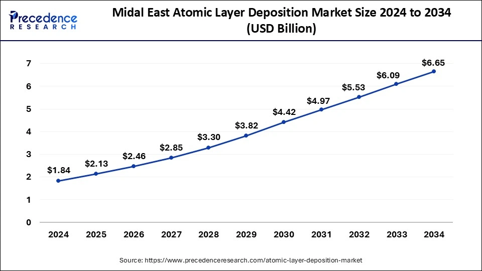
How is the Middle East & Africa Atomic Layer Deposition Market Expected to Grow from 2024 to 2034?
The Middle East & Africa atomic layer deposition market size is expected to grow from USD 2.13 billion in 2025 to approximately USD 6.65 billion by 2034. The industry is registering a notable CAGR of 13.48% from 2025 to 2034.
How the Middle East & Africa Dominated the Atomic Layer Deposition (ALD) Market?
The Middle East & Africa dominated the market in 2024. The growing expansion of the semiconductor industry, such as chip manufacturing, and high investment in solar energy, increases demand for ALD. The rising adoption of renewable energy and the development of high-quality electronic components increase demand for ALD. The growing advanced semiconductors & electronics industry and increasing adoption of electronics in various sectors like telecommunications, aerospace, & defense drive the overall growth of the market.
South Africa is a major player in the market due to its more advanced semiconductor research infrastructure, stronger presence of academic and industrial R&D institutions, and greater investment in nanotechnology and materials science. The country benefits from better access to skilled talent and technical resources, allowing it to adopt ALD technology in sectors like microelectronics, photovoltaics, and biomedical devices more effectively than other countries in the region. Additionally, government support for high-tech innovation, partnerships with global equipment suppliers, and a growing demand for high-precision thin-film coatings contribute to South Africa's leading position in the regional ALD market.
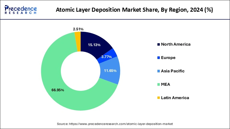
Why is North America Growing in the Atomic Layer Deposition Market?
North America is experiencing the fastest growth in the market during the forecast period. The growing advancements in semiconductor manufacturing and the miniaturization of electronic components increase demand for ALD. The increasing manufacturing of chips like FinFETs and 3D NAND requires ALD. The shift towards renewable energy and the high production of lithium-ion batteries increase demand for ALD. The increasing production of medical devices and the adoption of flexible electronic devices increase demand for ALD, supporting the overall growth of the market.
The U.S. is leading the regional market through its strong export presence, technological leadership, and global influence in semiconductor equipment manufacturing. Leading U.S.-based companies like Applied Materials, Lam Research, and Veeco Instruments supply cutting-edge ALD tools and technologies to MEA countries, which often lack local manufacturing capabilities. The U.S. maintains a competitive advantage by offering advanced, reliable ALD systems supported by deep R&D, strong intellectual property, and global service networks.
Atomic Layer Deposition Market Segmentation Outlook
Product Outlook
How the Aluminum Oxide Segment Dominated the Atomic Layer Deposition Market?
The aluminum oxide segment dominated the market in 2024. The growing semiconductor manufacturing and memory devices increase demand for aluminum oxide. The increasing development of solar cells and lithium-ion batteries increases the adoption of aluminum oxide. It offers excellent dielectric properties and strong barrier performance. The increasing adoption of flexible electronics and the need for protective coatings increase the adoption of aluminum oxide, driving the overall growth of the market.
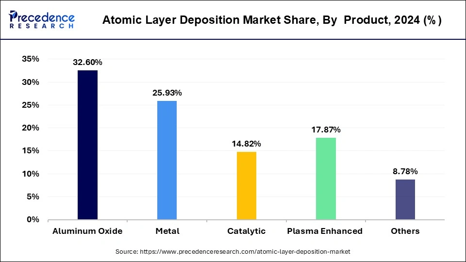
The plasma-enhanced segment is the fastest-growing in the market during the forecast period. The increasing manufacturing of 3D NAND memory and advanced memory & logic chips increases demand for PEALD. The growing advancements in energy storage systems and the development of photovoltaics increase demand for PEALD. It offers enhanced film quality and superior conformal coverage. It enhances film quality and greater precursor flexibility. The rise in electric vehicles and the expansion of 5G networks support the overall growth of the market.
Application Outlook
Which Application Held the Largest Share in the Atomic Layer Deposition Market?
The semiconductors segment held the largest revenue share in the atomic layer deposition market in 2024. The growing demand for semiconductors in sectors like AI, 5G, & IoT increases demand for ALD. The increasing manufacturing of metal gates, spacers, high-k dielectrics, and barriers increases the adoption of ALD.
The growth in data centers and the complexity in 3D chip design increase the adoption of ALD. The expansion of power electronics and the development of next-gen devices increase demand for semiconductors, driving the overall growth of the market.
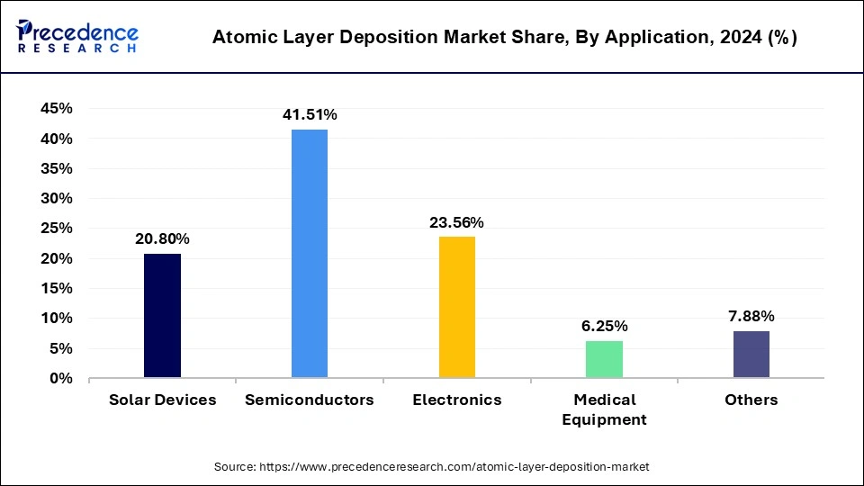
The solar devices segment is experiencing the fastest growth in the market during the forecast period. The increasing manufacturing of photovoltaic cells and the focus on sustainable energy increase demand for ALD. The growing manufacturing of solar panels and advancements in solar cell technology increase demand for ALD. The growing adoption of renewable energy and the expansion of solar technology increase demand for ALD, supporting the overall growth of the market.
Who Are the Key Players in the Atomic Layer Deposition Market?
- Lam Research Corporation - offers advanced atomic layer deposition (ALD) systems for high-volume semiconductor manufacturing with a focus on 3D scaling.
- Applied Materials, Inc. - provides cutting-edge ALD technologies integrated into its deposition platforms for advanced logic and memory devices.
- Tokyo Electron Ltd. - delivers precision ALD tools designed for ultra-thin film formation in next-generation semiconductor nodes.
- ASM International – a pioneer in ALD technology, offering single-wafer and batch ALD systems used in both front-end and back-end semiconductor processes.
- Veeco Instruments, Inc. - supplies ALD equipment optimized for compound semiconductors and advanced packaging applications.
- Denton Vacuum, LLC. - offers compact, customizable ALD solutions for R&D and low-volume production environments.
- Picosun Group - specializes in high-quality ALD systems for industries ranging from semiconductor and MEMS to medical and lighting.
- ALD NanoSolutions, Inc. - focuses on precision nanocoating solutions using ALD for a variety of materials and substrates.
- Beneq Oy - known for its industrial-scale and research-grade ALD equipment, especially in thin-film encapsulation and optical coatings.
- Kurt J. Lesker Company - provides customizable ALD systems designed for both research and light industrial use.
-
Canon Anvela Corporation (formerly known as Canon Tokki) - offers specialized ALD systems tailored for OLED and display applications.
What Are the Recent Developments in the Atomic Layer Deposition Market?
- In August 2024, Kalpana Systems launched roll-to-roll spatial atomic layer deposition tools. The tool is used in the manufacturing of organic LED, packaging, solar PV, and batteries. The company is developing two models, like the K600, for the packaging & battery sector, and the K300 for electronics and the solar sector. (Source: https://www.pv-magazine.com)
- In February 2025, Lam Research Ushers launched ALTUS Halo for Molybdenum atomic layer deposition for semiconductor metallization in Korea. It is widely used in chip manufacturing and the production of advanced semiconductors. (Source: https://newsroom.lamresearch.com)
Segments Covered in the Report
By Product
- Aluminium Oxide
- Metal
- Catalytic
- Plasma Enhanced
- Others
By Application
- Solar Devices
- Semiconductors
- Electronics
- Medical Equipment
- Others
By Region
- North America
- U.S.
- Canada
- Europe
- Germany
- UK
- France
- Italy
- Spain
- Sweden
- Denmark
- Norway
- Asia Pacific
- China
- Japan
- India
- South Korea
- Thailand
- Latin America
- Brazil
- Mexico
- Argentina
- Middle East & Africa
- South Africa
- UAE
- Saudi Arabia
- Kuwait
Thank you for reading. You can also get individual chapter-wise sections or region-wise report versions, such as North America, Europe, or Asia Pacific.
Immediate Delivery Available | Buy This Premium Research Report@ https://www.precedenceresearch.com/checkout/1295
You can place an order or ask any questions, please feel free to contact at sales@precedenceresearch.com | +1 804 441 9344
Stay Ahead with Precedence Research Subscriptions
Unlock exclusive access to powerful market intelligence, real-time data, and forward-looking insights, tailored to your business. From trend tracking to competitive analysis, our subscription plans keep you informed, agile, and ahead of the curve.
Browse Our Subscription Plans@ https://www.precedenceresearch.com/get-a-subscription
About Us
Precedence Research is a worldwide market research and consulting organization. We give an unmatched nature of offering to our customers present all around the globe across industry verticals. Precedence Research has expertise in giving deep-dive market insight along with market intelligence to our customers spread crosswise over various undertakings. We are obliged to serve our different client base present over the enterprises of medicinal services, healthcare, innovation, next-gen technologies, semi-conductors, chemicals, automotive, and aerospace & defense, among different ventures present globally.
Web: https://www.precedenceresearch.com
Our Trusted Data Partners:
Towards Healthcare | Towards Packaging | Towards Automotive | Towards Chem and Materials | Towards FnB | Towards Consumer Goods | Statifacts | Towards EV Solutions | Towards Dental | Nova One Advisor | Market Stats Insight
Get Recent News:
https://www.precedenceresearch.com/news
For the Latest Update Follow Us:
LinkedIn | Medium | Facebook | Twitter
✚ Related Topics You May Find Useful:
➡️ The global chemical vapor deposition market size was estimated at USD 24.46 billion in 2024 and is predicted to increase from USD 26.71 billion in 2025 to approximately USD 58.98 billion by 2034, expanding at a CAGR of 9.20% from 2025 to 2034.
➡️ The global compound semiconductor market size was worth around at USD 53.46 billion in 2024 and is expected to grow from USD 59.44 billion in 2025 to approximately USD 154.54 billion by 2034, expanding at a CAGR of 11.20% from 2025 to 2034.
➡️ The global physical vapor deposition (PVD) market size is accounted for USD 23.09 billion in 2024 and is anticipated to reach around USD 43.75 billion by 2034, growing at a CAGR of 6.60% from 2024 to 2034.
➡️ The global wafer processing equipment market size was valued at USD 9.22 billion in 2024 and is expected to hit around USD 16.24 billion by 2034, growing at a CAGR of 5.82% from 2025 to 2034.
➡️ The global semiconductor capital equipment market size accounted for USD 108.56 billion in 2024 and is predicted to increase from USD 116.00 billion in 2025 to approximately USD 210.58 billion by 2034, expanding at a CAGR of 6.85% from 2025 to 2034.
➡️ The global semiconductor gases market size accounted for USD 10.87 billion in 2024 and is predicted to increase from USD 11.69 billion in 2025 to approximately USD 22.49 billion by 2034, expanding at a CAGR of 7.54% from 2025 to 2034.
➡️ The global 2D materials market size was calculated at USD 2.57 billion in 2024 and is predicted to increase from USD 2.67 billion in 2025 to approximately USD 3.79 billion by 2034, expanding at a CAGR of 3.95% from 2025 to 2034.
➡️ The global compound semiconductor market size was worth around at USD 53.46 billion in 2024 and is expected to grow from USD 59.44 billion in 2025 to approximately USD 154.54 billion by 2034, expanding at a CAGR of 11.20% from 2025 to 2034.
➡️ The global polyolefin shrink film market size was calculated at USD 8.89 billion in 2024 and is projected to surpass around USD 12.55 billion by 2034, expanding at a CAGR of 3.51% from 2025 to 2034.

![]()
Legal Disclaimer:
EIN Presswire provides this news content "as is" without warranty of any kind. We do not accept any responsibility or liability for the accuracy, content, images, videos, licenses, completeness, legality, or reliability of the information contained in this article. If you have any complaints or copyright issues related to this article, kindly contact the author above.
